店名:進化系女裝男子喫茶IroHa Bar
地址:807 高雄市三民區建國二路109號2樓
電話:07-236 6362
營業時間:週日至週三為18:00~24:00
週五週六則為18:00~26:30
(每週四為公休日) 《本營業時間為2017.11更新》
價位範圍(每人):低消150元,無服務費,消費時間90分鐘。
未客滿時可加單延長時段。
可拍店內裝潢、餐點,不可拍到服務生。
官網:https://www.facebook.com/IROHABAR/
https://www.tukuyomi.net/ (月讀總官網)
菜單:http://diddykue.pixnet.net/album/photo/126082058
《2017.11版本,會不定期更換》
店在哪?怎麼去:高雄IroHa Bar(偽娘餐廳)月讀進化系女裝男子喫茶-1.外觀篇
http://diddykue.pixnet.net/blog/post/219880941
餐點照片及價錢:高雄IroHa Bar(偽娘餐廳)月讀進化系女裝男子喫茶-2.餐點篇
http://diddykue.pixnet.net/blog/post/219881808
行前須知及活動:高雄IroHa Bar(偽娘餐廳)月讀進化系女裝男子喫茶-3.Q&A篇
http://diddykue.pixnet.net/blog/post/219891822
店內互動及美照:高雄IroHa Bar(偽娘餐廳)月讀進化系女裝男子喫茶-4.使徒篇
http://diddykue.pixnet.net/blog/post/219947193
高雄IroHa Bar(偽娘餐廳)月讀進化系女裝男子喫茶-5.撩妹篇
http://diddykue.pixnet.net/blog/post/219989871
穿女裝體驗服務:食記:高雄IroHa Bar(偽娘餐廳)月讀進化系女裝男子喫茶-6.變裝篇
http://diddykue.pixnet.net/blog/post/220522623
酒不醉人人心醉:食記:高雄IroHa月讀進化系偽娘餐酒館-7.心醉篇
http://diddykue.pixnet.net/blog/post/220976679
清聖濁賢唯杜康:食記:高雄IroHa月讀進化系偽娘餐酒館-8.人醉篇
http://diddykue.pixnet.net/blog/post/221480895
上一頁下一頁

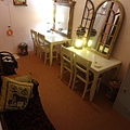
IroHa在二樓,會先在樓梯口看到放傳單的擺設桌,有朵散發香氣的玫瑰

桌子旁邊就是IroHa的門,準備進入新世界

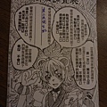
打開門會先看到這張桌子,下面有幾本日文版的漫畫周刊

門旁邊有一台很有特色的收音機,真的可以使用

鏡頭拉遠XD 收音機旁邊就是出租衣物架

各種款式,每件每次租借僅收60元洗衣費

往深處拍,跟2017相比變成電視在廚房旁邊,電視的功能主要是唱日K

可以把點歌機拿去座位上點歌,DAM機種精密採點增添樂趣(?

詢問之後店家同意讓我參觀拍攝一樓的更衣室
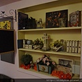
一進門右側的架子上擺滿有趣的飾品,果然很有月讀風格

往左看就是更衣區,紅色的布簾圍住魔法陣,變身出來的都是可愛的女孩紙

魔法陣旁有置物櫃,原本預計是可以出租給罪人的,但目前似乎暫緩

魔法陣旁邊是廁所,連廁所架上都堆滿了魔法書XD
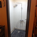
廁所隔壁是暫時不能使用的淋浴間...也許之後會開放XD
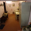
左邊的躺椅讓我很想把Hime公主抱放上去,灑上玫瑰花和緞帶拍張美照(不要妄想QQ
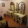
很有特色的造型梳妝台,還有地球儀造型的檯燈
燈愣~點燈後
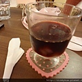
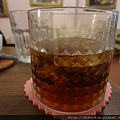
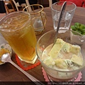
深海棲姬(紅酒 ICE) NT195

紅酒加上切丁的蘇打冰棒
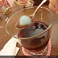
如果想喝酒味濃一點就速速撈起來吃掉

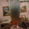
Mitiru告訴我這個是魔法燈,施展魔法就會亮起來唷

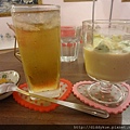
七大罪NT360
白俄羅斯NT250
黑俄羅斯NT250
使徒特調雞尾酒NT185
是Hime特地幫我做的!!!喝起來特別甜>////<攪拌後變成漂亮的紫色(可惜拍不太出來)
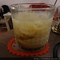
左:柚子梅酒NT235 右:摩耶(薄巧利口酒)NT230
這兩樣都很特別,柚子醬加入梅酒酸酸甜甜,摩耶感覺就是在吃淋上酒的雪糕XD
填寫意見表可以解業障集點卡的任務

我的集點之路還很遙遠QQ

IROHA特製叉燒飯NT75

叉燒肉很大塊很柔軟,挑出來拍一下
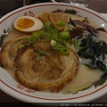
九州豚骨拉麵170元,這次湯的口味明顯比上次濃郁,有改配方嗎?@@
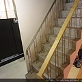
終於記得來拍2.5樓的廁所(左邊),右邊依稀可見二樓門口的傳單桌
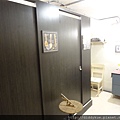
不分男女,是性別友善廁所
不知道為什麼裡面有三張椅子可以坐著休息XD

哆啦A夢的法寶:聲音凝固劑
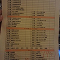
菜單全
菜單上
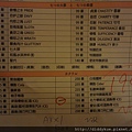
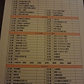
菜單下
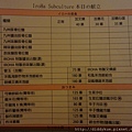
菜單全
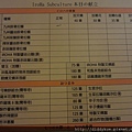
菜單上
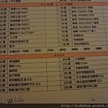
菜單下

Hime自由發揮拍了她覺得最美的照片,神氣質啊Q///Q

我指定的道具花,Hime微笑的嘴角甜到我要被甜甜滲透壓逼死了Q////Q

拍照用的道具花

25627164_1982211748771295_2424385599126657825_o

28311893_1630952620331480_547506997_o

興奮度120%


辛子燻雞冷盤NT125

警察叔叔就是這個人

上一頁下一頁
分享:


相片最新留言
此相簿內的相片目前沒有留言
此相簿內的相片出現在:
相簿列表資訊
- 最新上傳:
- 2018/03/01
- 全站分類:
- 電玩動漫
- 本日人氣:
- 0
- 累積人氣:
- 932

常見的半導體材料有矽、鍺、砷化鎵等
/
晶片測試
晶片處理高度有序化的本質增加了對不同處理步驟之間度量方法的需求。晶片測試度量裝置被用於檢驗晶片仍然完好且沒有被前面的處理步驟損壞。如果If the number of dies—the 積體電路s that will eventually become chips—當一塊晶片測量失敗次數超過一個預先設定的閾值時,晶片將被廢棄而非繼續後續的處理製程。
/
晶片測試
晶片處理高度有序化的本質增加了對不同處理步驟之間度量方法的需求。晶片測試度量裝置被用於檢驗晶片仍然完好且沒有被前面的處理步驟損壞。如果If the number of dies—the 積體電路s that will eventually become chips—當一塊晶片測量失敗次數超過一個預先設定的閾值時,晶片將被廢棄而非繼續後續的處理製程。
/
步驟列表
晶片處理
濕洗
平版照相術
光刻Litho
離子移植IMP
蝕刻(干法蝕刻、濕法蝕刻、電漿蝕刻)
熱處理
快速熱退火Annel
熔爐退火
熱氧化
化學氣相沉積 (CVD)
物理氣相沉積 (PVD)
分子束磊晶 (MBE)
電化學沉積 (ECD),見電鍍
化學機械平坦化 (CMP)
IC Assembly and Testing 封裝測試
Wafer Testing 晶片測試
Visual Inspection外觀檢測
Wafer Probing電性測試
FrontEnd 封裝前段
Wafer BackGrinding 晶背研磨
Wafer Mount晶圓附膜
Wafer Sawing晶圓切割
Die attachment上片覆晶
Wire bonding焊線
BackEnd 封裝後段
Molding模壓
Post Mold Cure後固化
De-Junk 去節
Plating 電鍍
Marking 列印
Trimform 成形
Lead Scan 檢腳
Final Test 終測
Electrical Test電性測試
Visual Inspection光學測試
Baking 烘烤
/
有害材料標誌
許多有毒材料在製造過程中被使用。這些包括:
有毒元素摻雜物比如砷、硼、銻和磷
有毒化合物比如砷化三氫、磷化氫和矽烷
易反應液體、例如過氧化氫、發煙硝酸、硫酸以及氫氟酸
工人直接暴露在這些有毒物質下是致命的。通常IC製造業高度自動化能幫助降低暴露於這一類物品的風險。
/
Device yield
Device yield or die yield is the number of working chips or dies on a wafer, given in percentage since the number of chips on a wafer (Die per wafer, DPW) can vary depending on the chips' size and the wafer's diameter. Yield degradation is a reduction in yield, which historically was mainly caused by dust particles, however since the 1990s, yield degradation is mainly caused by process variation, the process itself and by the tools used in chip manufacturing, although dust still remains a problem in many older fabs. Dust particles have an increasing effect on yield as feature sizes are shrunk with newer processes. Automation and the use of mini environments inside of production equipment, FOUPs and SMIFs have enabled a reduction in defects caused by dust particles. Device yield must be kept high to reduce the selling price of the working chips since working chips have to pay for those chips that failed, and to reduce the cost of wafer processing. Yield can also be affected by the design and operation of the fab.
Tight control over contaminants and the production process are necessary to increase yield. Contaminants may be chemical contaminants or be dust particles. "Killer defects" are those caused by dust particles that cause complete failure of the device (such as a transistor). There are also harmless defects. A particle needs to be 1/5 the size of a feature to cause a killer defect. So if a feature is 100 nm across, a particle only needs to be 20 nm across to cause a killer defect. Electrostatic electricity can also affect yield adversely. Chemical contaminants or impurities include heavy metals such as Iron, Copper, Nickel, Zinc, Chromium, Gold, Mercury and Silver, alkali metals such as Sodium, Potassium and Lithium, and elements such as Aluminum, Magnesium, Calcium, Chlorine, Sulfur, Carbon, and Fluorine. It is important for those elements to not remain in contact with the silicon, as they could reduce yield. Chemical mixtures may be used to remove those elements from the silicon; different mixtures are effective against different elements.
Several models are used to estimate yield. Those are Murphy's model, Poisson's model, the binomial model, Moore's model and Seeds' model. There is no universal model; a model has to be chosen based on actual yield distribution (the location of defective chips) For example, Murphy's model assumes that yield loss occurs more at the edges of the wafer (non-working chips are concentrated on the edges of the wafer), Poisson's model assumes that defective dies are spread relatively evenly across the wafer, and Seeds's model assumes that defective dies are clustered together.[25]
Smaller dies cost less to produce (since more fit on a wafer, and wafers are processed and priced as a whole), and can help achieve higher yields since smaller dies have a lower chance of having a defect. However, smaller dies require smaller features to achieve the same functions of larger dies or surpass them, and smaller features require reduced process variation and increased purity (reduced contamination) to maintain high yields. Metrology tools are used to inspect the wafers during the production process and predict yield, so wafers predicted to have too many defects may be scrapped to save on processing costs.[26]